| Specifications |
| Holder Type: |
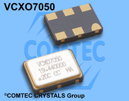
Voltage Controlled Crystal Oscillator CMOS/TTL
VCXO7050TF3.3-6pad 3.3V(Voltage code is "3.3"); Tri-State |
| Frequency Range: |
38.0 MHz to 640.0 MHz |
| Frequency Stability at 25°C: |
±25ppm (typ.) , ±50ppm, ±100ppm |
| Operating Temperature Range: |
-20°C to +70°C, -40°C to +85°C |
| Frequency Deviation Range: |
±80.0 ppm min. ±100ppm (typ.), ±150ppm |
| Storage Temperature: |
-50°C to +100°C |
| Power Supply Voltage (Vdd): |
+ 3.3V D.C. ± 5% |
| Maximum Supply Current (15pF load): |
< 100MHz : 30mA max., 100 MHz to 640 MHz : 50mA max.
|
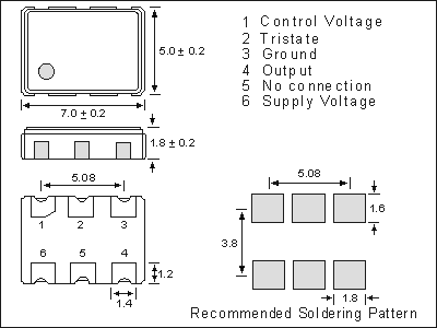
| Voltage Control: |
1.65V DC Center / 0.3V to 3.0V Range |
| Load: |
15pF |
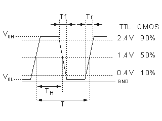
| Output Logic Levels: |
High "1" 90% of Vdd-min, Low "0" 10% Vdd-max.,
|
| Output Symmetry (Duty Cycle): |
50% ± 5%max. (measured at 50% Vdd) |
| Rise/Fall Time: |
0.7ns typical, (0.3V<->3.0V, 15pF load) |
| Start Up Time: |
10 ms (max.); 5 ms (typical) |
| Input Impedance: |
60 K? ( min.) |
| Linearity: |
6% typical, 10% max. |
| Tri-State Function: |
Tri-State Enable High. No connection or 70% of Vdd min. is applied to a Tri-state
pad to enable output. 30% of Vddmax. to disable outputs (high impedance). |
| Phase Jitter (12 kHz to 20 MHz): |
0.4 ps typ., 0.5 ps max., for 156.250MHz |
| Phase Noise (typical), Vcon :GND: |
(Offset 156.250 MHz)
-62dBc/Hz @ 10Hz, -92dBc/Hz @ 100Hz, -120dBc/Hz @ 1kHz
-132dBc/Hz @ 10kHz, -128dBc/Hz @ 100kHz, -140dBc/Hz @ 1MHz |
| Aging: |
< ±3ppm max. for the first year; 2ppm max. per year thereafter |
| Input Impedance: |
60 K? ( min.) |
| Reflow Condition: |
260°C max for 10 sec. |