| Specifications |
| Holder Type / Voltage (Vdd): |
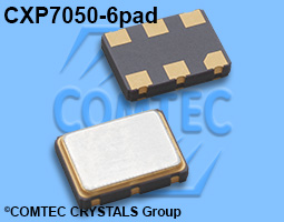
CXP7050DQF2.5; + 2.5V D.C. ± 5%; Tri-State on pad 1 |
| Frequency Range: |
10.000 MHz to 1500.000 MHz |
| Frequency Tolerance at 25°C: |
±20 to ±100 ppm |
| Operating-//Storage -Temperature Range: |
-20°C to +70°C, -40°C to +85°C // -55°C to +150°C |
| Maximum Supply Current (15pF load): |
100MHz: 16mA typical to 1.35GHz: 26mA typical;
|
| Output Logic: |
"High",1: 1.4V(typical); 1.6V (max.), RL = 100 Ohm
"Low ",0: 0.9V (min); 1.1V (typical), RL = 100 Ohm |
| Output Voltage Swing: |
250mV min., 350 typ., 450mV max., RL = 100 Ohm |
| Load: |
100 Ohm between output and complimentary output |
| Start Up Time: |
5 ms typical; 10ms max. |
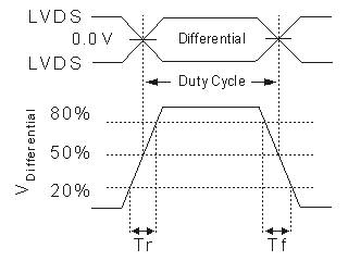
| Rise (Tr)/Fall Time (Tf): |
0.2ns typical; 0.5ns max. (20%Vdd<->80% of the LVDS wave form) |
| Output Enable Function: |
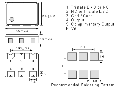
OE Control on Pad 1
70% of VDD (min.) to enable output. (Open connection prohibit.)
30% of VDD (max.) to disable output (high impedance). |
| Phase Jitter: |
1.0 ps typ. (12 kHz to 20 MHz); < 100 fs (1.875 MHz to 20MHz) |
| Phase Noise (156.250 MHz): |
-55dBc/Hz @ 10Hz, -85dBc/Hz @ 100Hz, -109dBc/Hz @ 1kHz
-116dBc/Hz @ 10kHz, -118dBc/Hz @ 100kHz, -139dBc/Hz @ 1MHz,
-146dBc/Hz @ 5MHz |
| Aging: |
< ±2ppm max. for the first year; ±10ppm max. over 10 years |
| Reflow Condition: |
260°C max for 10 sec. |