| Specifications - Product No. G371000000DECUPN43BB |
| Holder Type: |
CXO2520DK3.3; 3.3V(Voltage code is "3.3"); Tri-State on pad 1 |
| Frequency: |
371.000000 MHz |
| Frequency Stability at 25°C: |
± 50.0 ppm |
| Operating Temperature Range: |
± 50.0 ppm ; -40°C to +85°C (incusive of 25°C tolerance,
±10% input voltage variation, load change, aging, shock and vibration ) |
| Storage Temperature: |
-55°C to +150°C |
| Power Supply Voltage (Vdd): |
+ 3.3V D.C. ± 5% |
| Maximum Supply Current (15pF load): |
90.0 mA max. |
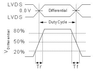
| Differential Output: |
Voltage, Vod: 247mV min; 355mV typical; 454mV max. Output1 - output 2
Error, dVod : -50mV min; 50mV max. |
| Output Voltage Swing: |
250 mV min; 350 mV typical; 450 mV max. RL=100Ohm |
| Output Logic Levels: |
High "1" 1.43V typical; 1.6V max, RL=100 ohms.;
Low "0" 0.9V min; 1.1V typical, RL=100 ohms |
| Offset Magnitude Error, (dVos): |
0mV min.; 3mV typical; 25mV max. |
| Output Offset Voltage, (Vos): |
1.125V min.; 1.200V typical; 1.375 V max. |
| Output Symmetry (Duty Cycle): |
50% ± 5%max. measured at 50% waveform |
| Load: |
RL=100 ohms between output and complimentary output |
| Rise/Fall Time: |
Tr = 0.2 ns. typ; 0.4 ns. max. 20% -> 80% of waveform
Tf = 0.2 ns. typ; 0.4 ns. max. 80% -> 20% of waveform |
| Start Up Time: |
± 3 ppm max. first year ; ± 2 ppm max. per year thereafter |
| Tri-state Function Pin 1: |
Enable ll When 70% min. of VDD to Enable Output. Enable time : 10 ms max.
Disable ll When 30% max. of VDD to Disable Output.
Disable current : 10 µA max. , Disable time : 0.2 µs max. |
| Phase Jitter (12 kHz to 20 MHz): |
0.2 ps typical, 0.5 ps (max.), for 156.250 MHz, 3.3V |
| Period Jitter, RMS, peak to peak: |
(decoupling capacitor between Vdd and GND) for 156.250 MHz
RMS: 3ps typ., 5ps max; peak to peak: 20ps typ; 30ps max. |
| Phase Noise (156.250 MHz): |
-50dBc/Hz @ 10Hz, -80dBc/Hz @ 100Hz, -115dBc/Hz @ 1kHz
-135dBc/Hz @ 10kHz, -142dBc/Hz @ 100kHz, -147dBc/Hz @ 1MHz,
-152dBc/Hz @ 10MHz |
| Aging: |
< ±3ppm max. for the first year |
| Reflow Condition: |
260°C max for 10 sec. |